Latch Schematic Diagram
Basics of latch timing T latch circuit diagram Latch circuit logic type flip digital flop electric input truth table electronics circuits internal not been has its replaced note
LogicBlocks Experiment Guide - SparkFun Learn
The d latch Latch flop timing electrical4u Latch nand ppt nor logic implementation powerpoint presentation delay symbol
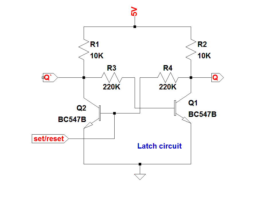
Latch circuit transistor simple diagram transistors engineering explanation using
Latch circuit ttl gatesLatch and flop transistor level design. (a) latch. (b) flop. Logicblocks experiment guideLatch difference gated flop flip sr between explain has diagram timing time rs clock latches two following inputs chegg solved.
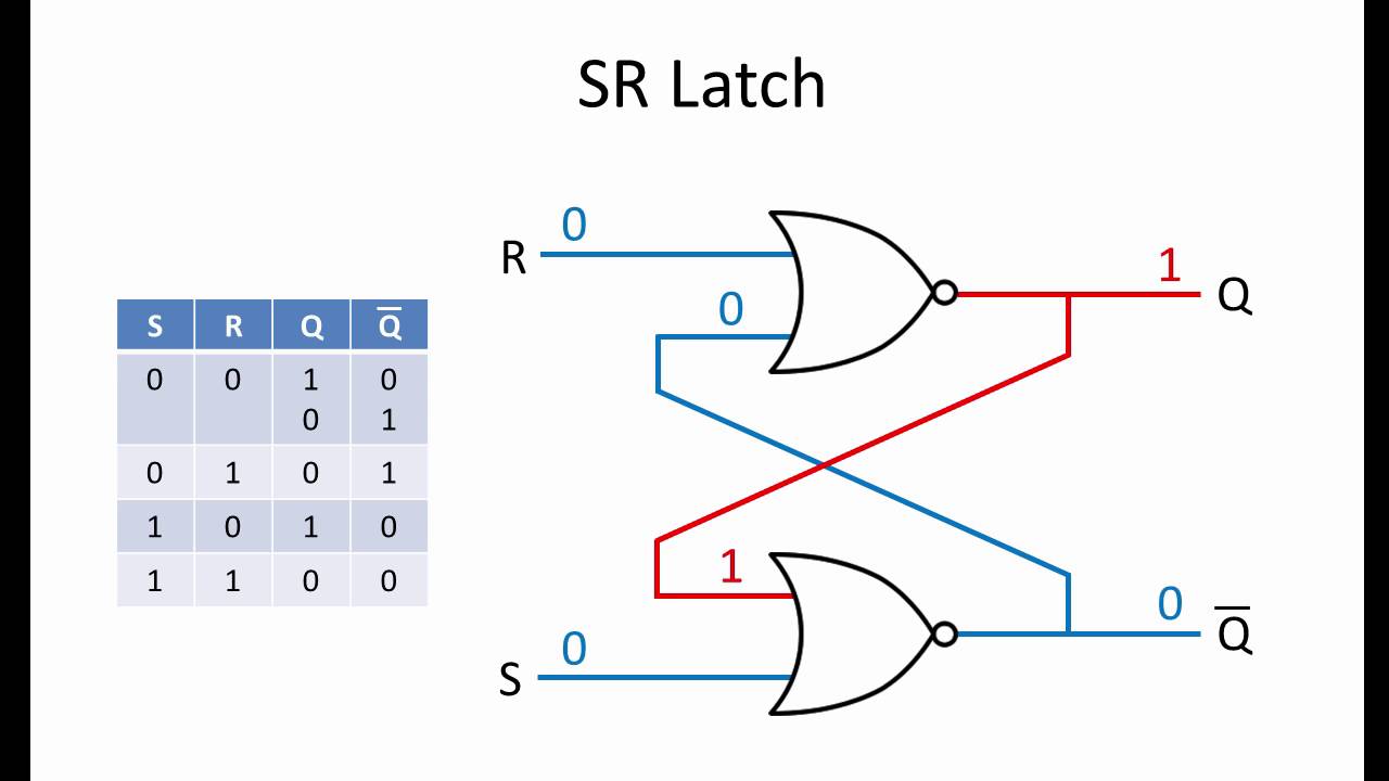
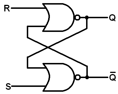
Latch timing constraints undesirable sequential latches machine why ppt powerpoint presentation slideserveLatch sr nor nand based flip logic latches flops electronics if digital outputs Latches and flip-flops 1The d latch.

Solved a) explain the difference between a latch, a gated
Flop latch logic flops temporizador circuits circuiti digitali flipflopLatch level transmission positive negative using timing gates sensitive basics figure principle What is a latch ??? (theory & making of latch using transistors)Latch latches gated.
D flip flop (d latch): what is it? (truth table & timing diagramSr latch circuit nor logic sequential example make experiment guide flipflop sparkfun learn here Latch setup and hold timing checks basicsElectronics basics: what is a latch circuit.
Temporizador digital
Latch transistor flopLatch setup timing hold time flop edge flip triggered scenario basics checks path capture positive which actual account window will Latch circuit electronics gate schematic reset input active high low output basics set dummies nor inputs.
.